

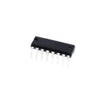
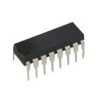
CD40109 CMOS Quad Low to High Voltage Level Shifter IC DIP-16 Package
CD40109 contains four low-to-high-voltage level-shifting circuits. Each circuit will shift a low-voltage digital-logic input signal (A, B, C, D) with logical 1 = VCC and logical 0 = VSS to a high-voltage output signal (E, F, G, H) with logical 1 = VDD and logical 0 = VSS. The RCA-CD40109, unlike other low-to-high level-shifting circuits, does not require the presence of the high-voltage supply (VDD) before the application of either the low-voltage supply (VCC) or the input signals. There are no restrictions on the sequence of application of VDD, VCC, or the input signals. In addition, with one exception there are no restrictions on the relative magnitudes of the supply voltages or input signals within the device maximum ratings, provided that the input signal swings between VSS and at least 0.7 VCC; VCC may exceed VDD, and input signals may exceed VCC and VDD. When operated in the mode VCC > VDD, the CD40109 will operate as a high-to-low level-shifter. The CD40109 also features individual three-state output capability. A low level on any of the separately enabled three-state output controls produces a high-impedance state in the corresponding output. This product is known as CD40109 IC Quad Low-to-High Voltage-Level Shifter, CD40109 Quad Low-to-High Voltage-Level Shifter, CD40109 Low to High Voltage Level Shifter, CD40109BPWE4,CD40109BE,CD40109BPW,CD40109BPWRG4,CD40109BNSR,CD40109BQNSRQ1,CD40109BPWR,CD40109BNSRE4,CD40109BPWRE4
Features:
- Qualified for Automotive Applications
- Independent of Power Supply Sequence Considerations
– VCC Can Exceed VDD
– Input Signals can Exceed Both VCC and VDD - Up and Down Level-Shifting Capability
- Three-State Outputs With Separate Enable Controls
- Standardized Symmetrical Output Characteristics
- 100% Tested for Quiescent Current at 20 V
- Maximum Input Current:
– 1 µA at 18 V Over Full - Package-Temperature Range
– 100 nA at 18 V and 25°C - Noise Margin (Full Package-Temperature
Range):
– 1 V at VCC = 5 V, VDD = 10 V
– 2 V at VCC = 10 V, VDD = 15 V - 5-V, 10-V, and 15-V Parametric Ratings
- Meets All Requirements of JEDEC Tentative
Standard No. 13B
Features/Specs:
- Logic Family: CD4010x
- Series: CD40109B
- Product Category: Translation – Voltage Levels
- Propagation Delay Time: 100 ns
- Operating Supply Voltage: 3 ~ 18V
- Power Dissipation: 500 mW (1/2 W)
- Data Rate: 10 Mb/s
- Features: Output enable, 20-V rated
- High Level Output Current: 6.8 mA
- Logic Type: Voltage Level Translator
- Low Level Output Current: 6.8 mA
- Operating Temperature Range: -55 ~ +125°C
- Mounting Style: Through Hole
- Package/Case: PDIP-16
- Weight: 1 gm
Applications:
- High-or-Low Level-Shifting With Three-State Outputs for Unidirectional or Bidirectional Bussing
- Isolation of Logic Subsystem Using Separate Power Supplies from Supply Sequencing, Supply Loss, and Supply Regulation Considerations
Package Includes:
- 1 x CD40109 CMOS Quad Low to High Voltage Level Shifter IC DIP-16 Package
Datasheet: CD40109B
Note: Product Images are shown for illustrative purposes only and may differ from the actual product.
Reviews
There are no reviews yet.